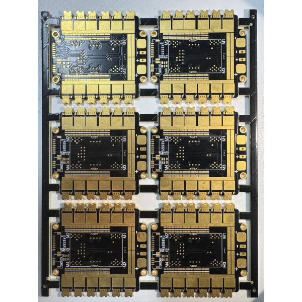
Product Description:
High Density PCBs (Printed Circuit Boards), or HDPCBs, are advanced
circuit boards characterized by high component density, fine line
widths/spacings (typically ≤ 0.1mm), small via sizes (e.g.,
microvias ≤ 0.15mm), and multi-layer structures. Their core
advantage lies in enabling miniaturization, high performance, and
reliabilityof electronic devices—making them indispensable in
industries where space constraints, signal integrity, and
functional complexity are critical.
Features:
1.Ultra-fine traces: Line widths/spacings ≤ 0.1mm (even down to
0.03mm), fitting more conductive paths in limited space.
2. Microvias: Tiny holes (≤0.15mm diameter) in blind/buried/stacked
designs, connecting layers without wasting surface area.
3. Multi-layer structure: 8–40+ layers (vs. 2–4 for traditional
PCBs) to isolate signals/power and integrate complex circuits.
4. High component density: ≥100 components per square inch,
enabling mini devices (e.g., smartwatches) with rich functions.
5. Specialized materials: High-Tg FR-4 (heat-resistant), polyimide
(flexible), or PTFE (low signal loss) for harsh environments/high
frequencies.
6. Strict precision: Tight tolerances (e.g., ±5% line width error,
≤0.01mm layer alignment) to avoid defects in fine structures.
7. Advanced component compatibility: Supports fine-pitch BGA, CSP,
and PoP packages, maximizing vertical/horizontal space use.
Applications:
| Sector | Use Cases | HDI Advantage |
|---|
| Consumer | Smartphones, AR/VR headsets | 50% size reduction vs. conventional PCBs |
| AI/Computing | GPU accelerators, server GPUs | Supports 25 Tbps/mm² interconnect |
| Medical | Endoscopic capsules, hearing aids | Reliability in 50 GHz) for signal integrity validation. |
HD PCB development trend in 2025
3D Heterogeneous Integration
- Chiplet Ecosystems: Hybrid bonding (e.g., TSMC’s CoWoS-L) with 8µm
line/space for NVIDIA/AMD GPU substrates.
- Silicon Interposers: TSV density >50k vias/mm², slashing signal
delay by 30% in AI servers.
- Embedded Actives: Bare dies integrated into PCB layers (e.g.,
Medtronic’s neural implants).